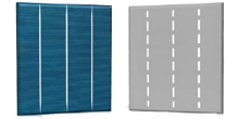
PV cells production
Production Lines perform 156 x156 mm polycrystalline Wafers carrying out the following phases:
- Wafer Optical Inspection: through robotized optical system, damaged wafer were isolated before processing thus maximizing the efficiency of the following phases.
- Superficial texturing: through the use of Hydrofluoric and nitric acids, it allows to make on the wafer a surface that maximized the capture of sunny radiation:
- Doping and diffusion: in this step is realized the N-P junction that allow cells to work. This step involves deposition of ortho-phosphoric acid controlled by ultrasound and phosphorus diffusion in Sylicon at high temperature by a furnace in continuous loop.
- Edge Insulation: in this phase is removed the residue ( called glass phosphor) products in the previous phase through a series of acid and basic baths. The insulation is separated by chemical way allowing the use of the energy produced.
- Anti reflex treatment: in this step a thin layer of Sylicon nitride is deposited so allowing to control the thickness with high precision thanks to the PECVD technique.
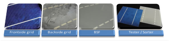
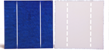
- Manufacture of electrodes: it is realized by depositing Aluminium and Silver metallization on the two sides of a cell in order to collect the electrical charges produced thus avoiding losses.
- Classification: in this phase cells are measured one by one in order to characterize their electrical parameters and to test their functioning before their packaging and delivery.
Product transformationCluster 1: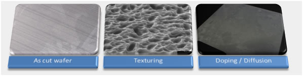 Cluster 2:
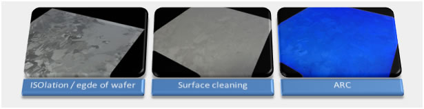 Cluster 3/4